17/02/24

Semiconductor housing components are complex critical parts requiring the unparalleled properties
of dimensional stability that Invar is known for.
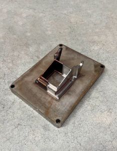
This nickel-iron alloy gets its name thanks to its extremely low coefficient of thermal expansion, from -250°C up to about 200°C. This feature makes it an ideal choice for measuring equipment, cryogenic applications, components for the semiconductor industry, and molds for the manufacturing of composite components for aerospace use.
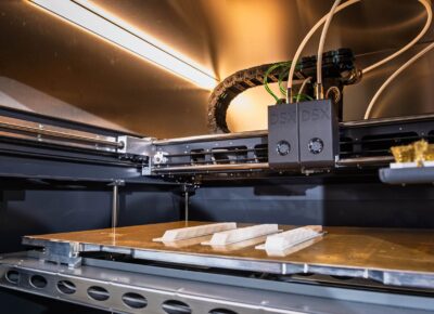
The semiconductor housing could be manufactured by CNC machining, scrapping about 75% of the mass of the initial steel stock. Additive manufacturing of the part via Melo LMD process allows the optimization of the material used. Fast design iteration and manufacturing flexibility are achieved, and only finishing steps by precision machining are required to obtain the final component.
 FR
FR